الصفحة الرئيسية

22/1/2018

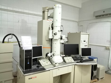
A Transmission Electron Microscope (TEM) provides ultra-high-resolution imaging by transmitting electrons through thin samples to reveal internal structures at the atomic or nanometer scale. Its output consists of detailed images showing morphology, crystallography, and defects in materials or cells. TEMs are widely applied in nanotechnology, biology, materials science, and semiconductor research. They are primarily used by researchers, advanced laboratories, and industrial R&D centers. Commercially, TEMs are essential in the electronics industry for chip failure analysis, in pharmaceuticals for drug delivery research, and in nanomaterials companies to validate product quality.

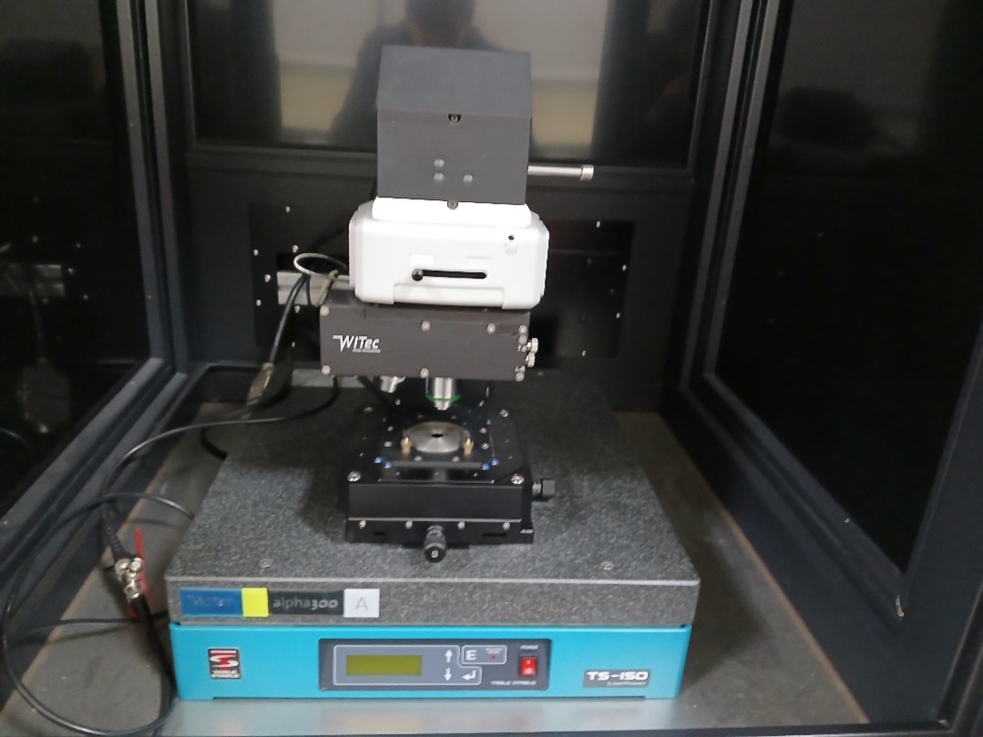
An Atomic Force Microscope (AFM) measures surface topography at the nanoscale by scanning a sharp tip over a sample surface and detecting interaction forces. Its outputs are 2D and 3D surface maps that reveal roughness, texture, and mechanical properties. AFM applications include material characterization, polymer science, biological imaging, and nanomanufacturing. Targeted users include nanoscience researchers, surface engineers, and biotechnology companies. Commercially, AFMs are used for quality assurance in microelectronics, nanocoatings, and medical implants, where precise surface analysis is crucial.

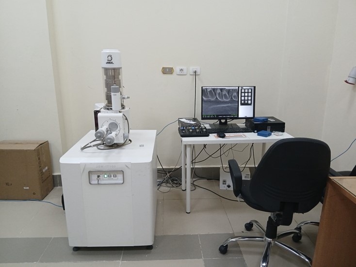
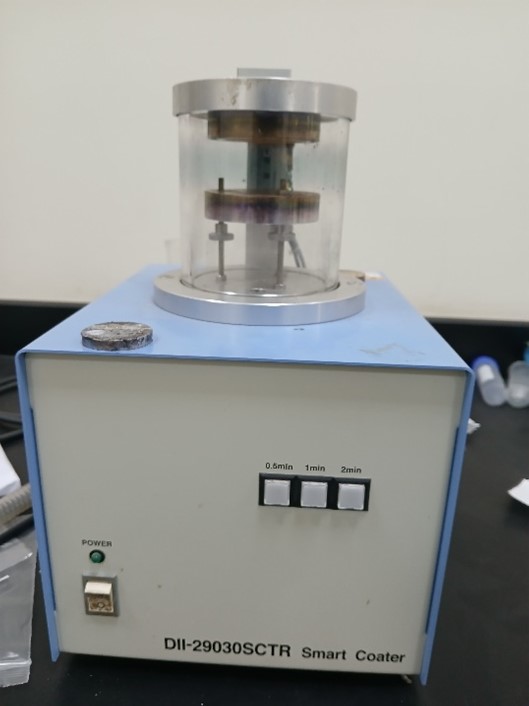
 A Scanning Electron Microscope (SEM) generates high-resolution images of surface structures by scanning a sample with an electron beam and detecting emitted signals. Its output includes detailed micrographs showing surface morphology, composition (via EDS attachments), and topographical contrast. SEM is widely used in metallurgy, forensics, geology, and biological sciences. Users include research institutes, manufacturing industries, and quality control laboratories. Commercially, SEM is integral to failure analysis in electronics, forensic investigations, and materials testing in aerospace and automotive sectors.

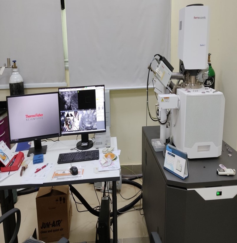
A Field Emission Electron Microscope (FE-SEM) is an advanced SEM that uses a field emission electron source to achieve superior resolution and image clarity. Its outputs are high-definition micrographs that reveal nanoscale surface features with high contrast. Applications include nanomaterials research, semiconductor inspection, and biomaterials analysis. FE-SEMs are mainly used by high-end research labs, nanotechnology companies, and semiconductor manufacturers. Commercially, they support industries requiring nanoscale precision, such as integrated circuits, advanced coatings, and catalyst development.

A Nitrogen Generator produces high-purity nitrogen gas from ambient air using membrane separation or pressure swing adsorption technology. The main output is a continuous supply of nitrogen suitable for laboratory and industrial use. Applications include providing inert atmospheres, preserving biological samples, and preventing oxidation during material processing. Typical users are laboratories, chemical industries, and food packaging companies. Commercially, nitrogen generators are used in pharmaceuticals, electronics, and food industries for cost-effective, on-demand nitrogen supply, replacing expensive bottled gases.